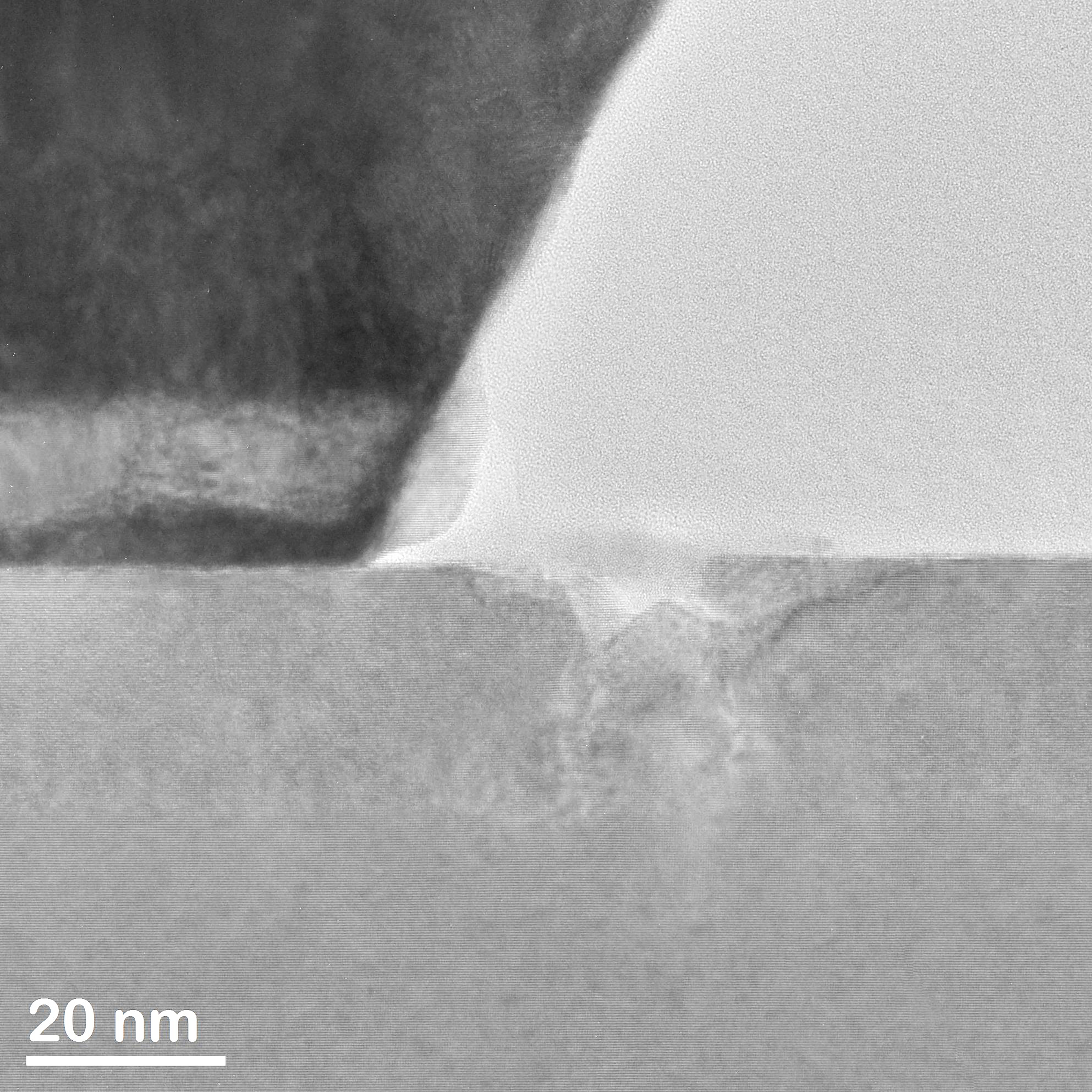
Energy-efficient chips based on the semiconductor material gallium nitride (GaN) are being developed by 26 partners from nine European countries in the project UltimateGaN. The Fraunhofer Institute for the Microstructure of Mate-rials and Systems IMWS in Halle (Saale) is one of the project’s partners, sharing its know-how in error diagnostics and the development of analytical methods. At a meeting held in Lausanne the project partners presented their first results.

Digitalization in industry and private households, electrification for enhancing mobility and the increased use of electricity from renewable energies generate the need for power semiconductors that are capable of converting electricity more efficiently than previous solutions. In order to make available this technology for a range of applications at competitive prices, 26 partners came together in UltimateGaN (Research for GaN technologies, devices and applications to address the challenges of the futureGaN roadmap), one of Europe’s largest research projects. They have placed their hopes on gallium nitride (GaN), a new semiconductor material, to enable use of innovative power and high-frequency electronics technology and hence the development of a new generation of energy-efficient chips. The possible applications of these new energy-efficient chips are myriad and include for example shorter charging times for electric vehicles, quicker data transfers between plants, buildings and machines or more efficient grid feed-ins of electricity from renewable energies.
For its part, the Fraunhofer IMWS brings many years of experience in high-resolution microstructure analysis and complex error diagnostics for electronic components, together with its know-how in the development of new study methods. The foundations of the project initiated in May 2019, with a duration of three years and which is led by Infineon Austria, were laid in the preceding research project PowerBase in which the research team from Halle was also involved.
“The base generation and the pilot line developed in the preceding project will now be taken to a new technological level. By further miniaturizing chips, increasing quality and lowering production costs, the aim is to exploit the global market potential of this technology. New materials such as gallium nitride require new approaches in error diagnostics, so as to be able to recognize, comprehend and hence rely on specific failure modes or degradation processes”, says Frank Altmann, Head of the Business Division “Electronics Materials and Components”.
The special material properties of GaN, which enable higher power densities, are the key to more efficient components. Components based on GaN can be housed in smaller and lighter component structures, enabling electricity to be switched more efficiently and higher data transmission rates. Power losses are reduced by up to one half. “High electrical field strengths and current and power densities in extremely compact components represent a particular challenge”, says Altmann. This is why the competencies of many partners have been pooled in Ultimate GaN, enabling the entire value chain to be covered, from process development, design, assembly and interconnection technologies, right down to integrated system solutions.
The work by the Fraunhofer IMWS centers on structure characterization and high-resolution error analytics of lateral and vertical GaN architectures and contributes to a deeper understanding of error modes and degradation mechanisms. This includes the characterization of interface properties at gate and ohmic contacts and between GaN stack and passivation, the development of specially adapted analytical methods enabling the localization and physical analysis of defects and the determination of defect risks in wire bonding over active GaN structures.
UltimateGaN is financed with investments from industry, grants from the German federal states involved and the ECSEL Joint Undertaking (Electronic Components and Systems for European Leadership).
UltimateGaN
https://www.ultimategan.eu/