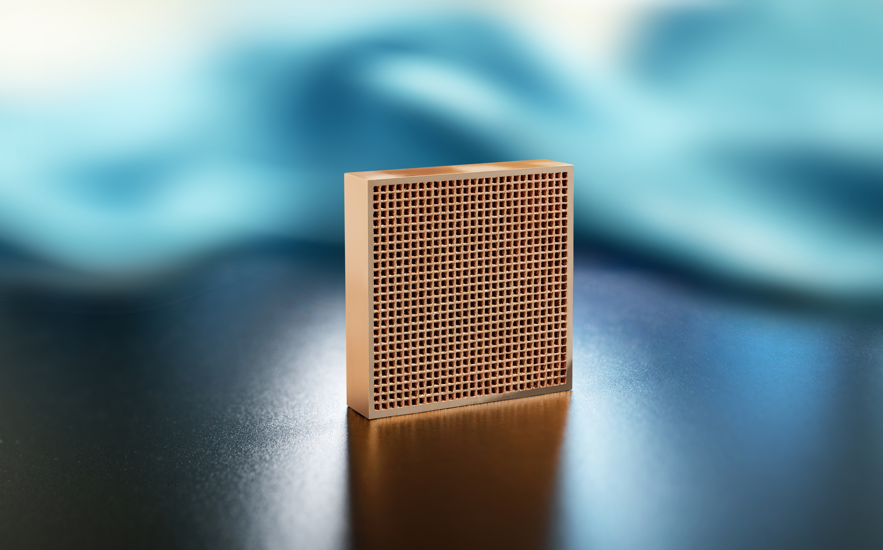
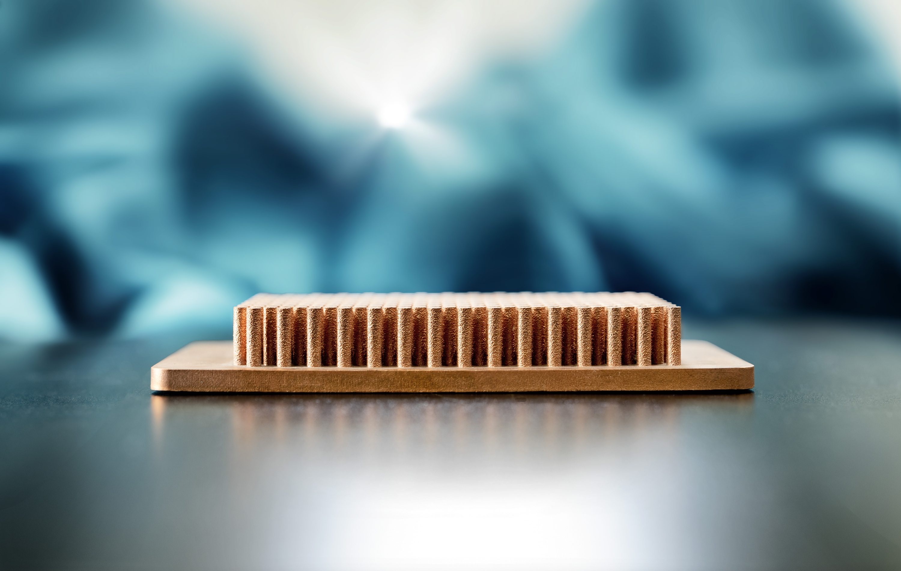
3D printed highly thermally conductive copper components as high-performance heatsinks
Easier processing, faster production times, high feasibility of short-term changes, reduced material consumption, increased functionality and thus reduced costs: Additive manufacturing processes open up more and more areas of application and are becoming increasingly relevant for industry. In a new project Fraunhofer Institute for Microstructure of Materials and Systems IMWS together with the copper semi-finished products manufacturer KME, are going to explore the use of additive manufacturing technologies for highly thermally conductive components made of copper and copper alloys. The aim is to open up new market segments in the field of cooling elements for power electronics.


Copper exhibits avery high thermal conductivity which is only surpassed by silver. Since silver - due to its significant price - is only used as a material in special cases, project partners in the joint project »Technology and Material Development for the additive production of complex high-heat conductive Cu components - CuAdd« will completely rely on copper and its alloys. Research into additive manufacturing methods based on copper is a market with highly attractive future prospects.
The project partners will evaluate additive manufacturing processes for metallic components, including Fused Deposition Modeling (FDM), Binder Jetting (BJ), Nano Particle Jetting (NPJ) and Laser Powder Bed Fusion (LPBF). In such technologies components are generated layer by layer. Copper or copper alloys are used as starting materials, which are available as pure powder or bound in filaments. These differ in further processing in the process-dependent material feed and in the processing temperature.
The preferred method of the researchers is the Laser Powder Bed Fusion (LPBF), as it is the most successful additive manufacturing process for the prototyping of metallic components to date. Here, the material is applied in powder form in a thin layer on a base plate. The powdered material is completely melted by defined laser radiation at temperatures above 1000 ° Celsius and forms a solid material layer. The plate is then lowered and powder reapplied. This cycle is repeated until all layers are melted and the component is finished.
»In addition to researching and evaluating the most suitable process for highly thermally conductive copper components, we will also examine which powder or powder mixture is suitable for which application due to its components. Factors such as particle size, flowability and porosity play an important role in achieving the desired properties such as high thermal conductivity or high electrical conductivity of the components,« explains Dr. Olaf Schwedler, Head of Process Development at the KME site in Hettstedt.
In the joint project, the copper grades Cu-ETP, Cu-OFE and Cu-HCP and the copper alloys CuCrZr and CuNi2SiCr will be tested. At the same time, the compatibility of different polymer systems such as PLA (polylactic acids) and PA (polyamide) with copper systems will be investigated.
»As a result, we want to produce a prototype with a geometrically complex structure using additive manufacturing processes that can be used, for example, as high-performance heat sink. If successfully implemented, conventional technologies which are complex and costly could be replaced step by step. We combine KME's industrial expertise in copper production with our competences of applied microstructure diagnostics and will thus enable a rapid development of expert knowledge in the field of copper powder production for 3D printing,« says Sandy Klengel, who is in charge of the project at Fraunhofer IMWS.